

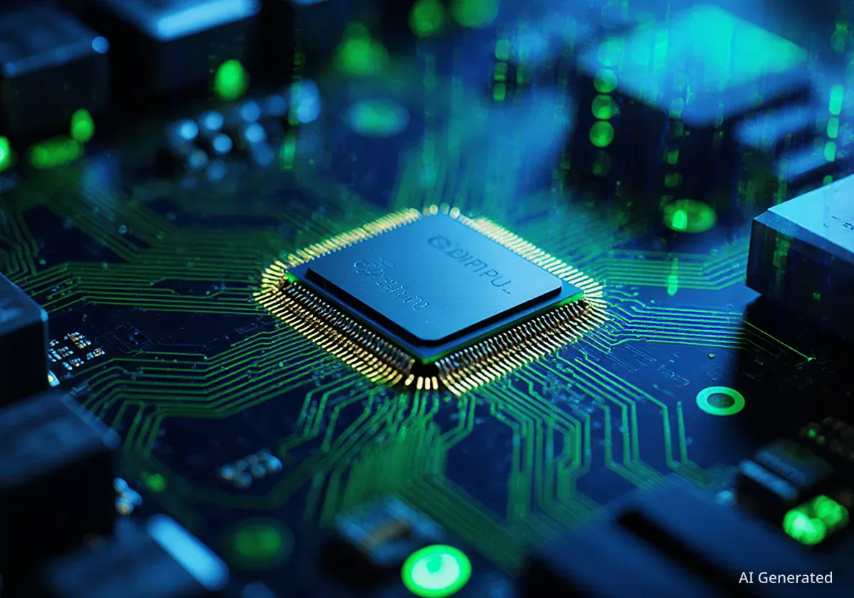


Taiwan Semiconductor Manufacturing Company's (TSMC) annual Open Innovation Platform (OIP) Ecosystem Forum showcased significant progress in semiconductor design, with a clear focus on artificial intelligence (AI) and chiplet technologies. Key electronic design automation (EDA) partners, including Cadence, Siemens EDA, and Synopsys, presented new tools and workflows aimed at accelerating the development of next-generation high-performance computing (HPC) and AI chips.
The event, held in Santa Clara, California, underscored the deep collaboration between TSMC and the EDA industry to support advanced manufacturing processes and complex packaging solutions. These partnerships are crucial for making sophisticated multi-die chiplet designs a commercial reality for a wider range of companies.
Key Takeaways
- Artificial intelligence and chiplet-based designs were the central themes at the TSMC OIP Ecosystem Forum 2025.
- Top EDA firms Cadence, Siemens EDA, and Synopsys revealed new design tools optimized for TSMC's latest technologies.
- Advancements focus on TSMC's N2 process node and its 3DFabric advanced packaging platform.
- The collaborations aim to improve design efficiency, performance, and power consumption for complex AI and HPC chips.
- These new tools are making advanced chiplet technology more accessible beyond industry giants like AMD, Intel, and Nvidia.
AI Integration in Chip Design Flows
A primary focus at the forum was the integration of artificial intelligence into the chip design process itself. EDA companies are developing AI-driven software to automate complex tasks, improve efficiency, and optimize chip performance for power, performance, and area (PPA).
Cadence AI-Driven Solutions
Cadence Design Systems presented its AI-powered design solutions, which have been validated for TSMC's N2 process node. These tools include features like automated design rule check (DRC) violation fixing, which helps engineers resolve design issues more quickly. This capability is expected to shorten the development cycle for AI chips manufactured on TSMC's most advanced processes.
The company also highlighted its Innovus+ AI assistant. This platform integrates synthesis and implementation into a single, AI-driven workflow, helping to achieve better PPA results and manage the complexity of modern chip designs.
Siemens EDA and Synopsys AI Initiatives
Siemens EDA demonstrated how its Calibre Vision AI software can improve productivity. The AI-powered tool analyzes and prioritizes DRC violations, allowing design teams to focus on the most critical issues first and streamline the debugging process.
Synopsys announced a collaboration with TSMC on silicon photonics. Their joint effort is creating an AI-optimized design flow for TSMC's Compact Universal Photonic Engine (COUPE) technology. This is designed to enhance system performance by addressing thermal and multi-wavelength challenges in multi-die AI systems that rely on high-speed optical connections.
Democratizing Chiplet Design
The collaborative efforts between TSMC and EDA partners aim to lower the barrier to entry for chiplet-based designs. By providing certified and automated toolchains, smaller companies can now explore multi-die architectures that were previously only feasible for large corporations with extensive resources.
Advancements in Chiplet and 3D-IC Technology
Alongside AI, chiplets and multi-die packaging were a dominant topic. As single-chip scaling becomes more challenging, the industry is moving toward combining multiple smaller dies, or chiplets, into a single package. This requires sophisticated design tools and advanced packaging technologies.
What is 3DFabric?
TSMC's 3DFabric is a comprehensive family of 3D silicon stacking and advanced packaging technologies. It includes solutions like System on Integrated Chips (SoIC) for direct die stacking, Chip on Wafer on Substrate (CoWoS) for integrating high-bandwidth memory, and Integrated Fan-Out (InFO) for high-density interconnects. These technologies enable the creation of powerful, integrated systems from multiple chiplets.
New Tools for Multi-Die Integration
Cadence confirmed that its 3D-IC solutions now support TSMC's 3DFabric platform across the N3, N2, and upcoming A16 process nodes. The company is working closely with TSMC on critical aspects of multi-die design, including bump connections and the physical implementation and analysis of multiple chiplets.
Siemens EDA has also enabled a design flow for TSMC's COUPE technology and has had its Calibre software certified for thermal and physical verification of TSMC's 3DFabric technologies. Its Innovator3D IC tool provides an automated workflow for TSMC's InFO packaging, simplifying a complex process for designers.
"The advancements in AI and chiplet realms are intertwined, paving the way for high-performance AI and HPC chips that serve compute-intensive workloads."
Synopsys showcased its 3DIC Compiler, a platform designed to manage the entire multi-die design process from exploration to final signoff. It supports TSMC's SoIC-X technology and automates complex routing for standards like UCIe and High-Bandwidth Memory (HBM), which are essential for connecting chiplets.
The Future of Semiconductor Design
The announcements at the TSMC OIP Ecosystem Forum 2025 provide a clear roadmap for the semiconductor industry. The convergence of AI-driven design automation and advanced chiplet packaging is set to define the next generation of computing hardware.
These collaborations are essential for several reasons:
- Managing Complexity: Modern AI chips can contain billions of transistors and require intricate multi-die configurations. AI-powered tools are necessary to manage this complexity.
- Improving Time-to-Market: Automation and improved efficiency in the design process help companies bring new products to market faster.
- Enabling Innovation: By providing robust toolchains for chiplets and 3D stacking, TSMC and its partners are enabling new system architectures that can deliver significant performance and efficiency gains.
As compute-intensive workloads in AI and HPC continue to grow, the innovations presented by TSMC, Cadence, Siemens EDA, and Synopsys will be fundamental to building the powerful and efficient processors required to meet future demand.